Login or Register for FREE!
Subelement E7

PRACTICAL CIRCUITS

Section E7B

Amplifiers: class of operation; vacuum tube and solid-state circuits; distortion and intermodulation; spurious and parasitic suppression; switching-type amplifiers

For what portion of the signal cycle does each active element in a push-pull, Class AB amplifier conduct?

  • Correct Answer
    More than 180 degrees but less than 360 degrees
  • Exactly 180 degrees
  • The entire cycle
  • Less than 180 degrees

As the name indicates, class AB amplifiers operate somewhere between class A and class B. Or perhaps the name is short for "Almost B" -- which would be true as well.

A class A amplifier operates at a full 360 degrees. The purity of amplification is terrific, but the efficiency is not.

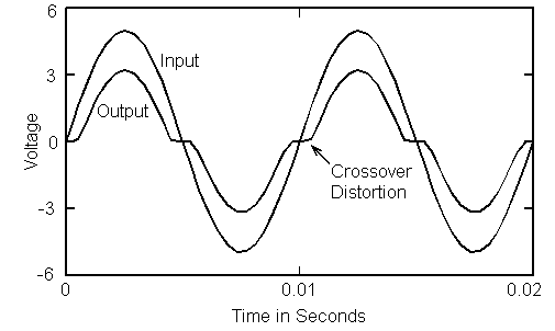
Class B amplification uses two "finals", each operating for 180 degrees of the wave -- a great improvement in efficiency. However, with the introduction of bipolar transistors as finals, a problem with class B amplification developed. In a pure class-B configuration, there is a period of time where neither the forward-going nor the negative-going final has a forward-biased base-emitter junction. When this type of amplifier is fed a pure sine wave, there is a "hitch" at the zero crossing caused by neither final being forward-biased. This is called crossover distortion, and is a highly undesirable alteration of a pure sine wave.

Crossover
Distortion

The simple and elegant solution to this was to bias the finals so that each one operates slightly more than 180 degrees (but less than 360 degrees) to eliminate the problem of crossover distortion. The result is an amplifier with "Almost Class B" efficiency, but with distortion characteristics close to class A. Or, as it is called, Class AB.

Last edited by orochimaru. Register to edit

Tags: none

What is a Class D amplifier?

  • Correct Answer
    An amplifier that uses switching technology to achieve high efficiency
  • A low power amplifier that uses a differential amplifier for improved linearity
  • An amplifier that uses drift-mode FETs for high efficiency
  • An amplifier biased to be relatively free from distortion

Just remember that the key feature of Class D amplifiers is high efficiency.

Each one of the wrong answers misleads you by putting the letter D in the description: differential, drift-mode, and doubling.

Trick: Class D, D is for Digital -> Technology is the answer.

Last edited by phongn. Register to edit

Tags: none

What circuit is required at the output of an RF switching amplifier?

  • Correct Answer
    A filter to remove harmonic content
  • A high-pass filter to compensate for low gain at low frequencies
  • A matched load resistor to prevent damage by switching transients
  • A temperature compensating load resistor to improve linearity
This question does not yet have an explanation! Register to add one

Tags: none

What is the operating point of a Class A common emitter amplifier?

  • Correct Answer
    Approximately halfway between saturation and cutoff
  • Approximately halfway between the emitter voltage and the base voltage
  • At a point where the bias resistor equals the load resistor
  • At a point where the load line intersects the zero bias current curve

Setting the bias half-way between saturation and cutoff gives the maximum possible swing in collector voltage without entering either saturation or cut- off.

Last edited by orochimaru. Register to edit

Tags: none

What can be done to prevent unwanted oscillations in an RF power amplifier?

  • Tune the stage for minimum loading
  • Tune both the input and output for maximum power
  • Correct Answer
    Install parasitic suppressors and/or neutralize the stage
  • Use a phase inverter in the output filter

Unwanted oscillations are also called parasitic oscillations. Naturally, a parasitic suppressor suppresses parasitic oscillations.

SWR, power, and phase are all more or less unrelated to oscillation.

Silly Hint: Parasites are unwanted

Last edited by sympathique. Register to edit

Tags: none

What is a characteristic of a grounded-grid amplifier?

  • High power gain
  • Correct Answer
    Low input impedance
  • High electrostatic damage protection
  • Low bandwidth

Memory Aid: The ground is under your feet so it is low and won't impede your walk.


Compare to transistor base, collector, emitter. Which common lead type has low impedance? Which lead is like the grid in a vacuum tube?

Last edited by wileyj2956. Register to edit

Tags: none

Which of the following is the likely result of using a Class C amplifier to amplify a single-sideband phone signal?

  • Reduced intermodulation products
  • Increased overall intelligibility
  • Reduced third-order intermodulation
  • Correct Answer
    Signal distortion and excessive bandwidth

From Wikipedia: "Class-C amplifiers conduct less than 50% of the input signal and the distortion at the output is high". So, the option that mentions distortion is correct.

Silly hint: Class C - correct answer contains words starting with the next letters in the alphabet; signal distortion and excessive bandwidth. (c, d, &e).

Last edited by jaeger21. Register to edit

Tags: none

Why are switching amplifiers more efficient than linear amplifiers?

  • Switching amplifiers operate at higher voltages
  • Correct Answer
    The switching device is at saturation or cutoff most of the time
  • Linear amplifiers have high gain resulting in higher harmonic content
  • Switching amplifiers use push-pull circuits

Linear amplifiers (such as Class A amps) bias transistors in their linear region. Whenever these transistors are conducting they are never fully on nor off, but have some instantaneous resistance which generates heat.

An ideal switch when closed has 0 ohms of resistance, and when open has infinite resistance. In either case the switch does not generate any heat.

Transistors in switching amplifiers act much like switches--they are either on or off most of the time. Because switched transistors are seldom partially on they don't generate much heat, resulting in low power dissipation compared to transistors operating in their linear region.

Hint: 'linear' descriptor of time, only answer with 'time'

Hint: The only one that doesn’t say amplifier

Last edited by antoszewski. Register to edit

Tags: none

What is characteristic of an emitter follower (or common collector) amplifier?

  • Low input impedance and phase inversion from input to output
  • Differential inputs and single output
  • Acts as an OR circuit if one input is grounded
  • Correct Answer
    Input and output signals in-phase
This question does not yet have an explanation! Register to add one

Tags: none

In Figure E7-1, what is the purpose of R1 and R2?

  • Load resistors
  • Correct Answer
    Voltage divider bias
  • Self bias
  • Feedback

R1 and R2 perform a simple voltage divider circuit. This allows the base of the bipolar junction transistor (BJT) to be fixed at a specific DC voltage.

Memory Hint: Picture R1 over R2 like a mathematic equation, R1 divided by R2.

Last edited by ki4myd. Register to edit

Tags: none

In Figure E7-1, what is the purpose of R3?

  • Fixed bias
  • Emitter bypass
  • Output load resistor
  • Correct Answer
    Self bias

Self-Biasing A.K.A. Transistor Biasing is the process of configuring a transistor's DC operating voltage/current conditions to the correct level so that any Alternating Current (AC) input signal can be amplified appropriately by the transistor.

Also, this assists with elimination of clipping.

Hint: R3 is sitting down there all by itSELF.

TEST TIP: Being in the horizontal center of the diagram near the bottom edge of the page, the resistor looks like it is pointing at you. Therfore, remember R3 as the "pointing at yourSELF BIAS RESISTOR."

Last edited by w9mpx. Register to edit

Tags: none

What type of amplifier circuit is shown in Figure E7-1?

  • Common base
  • Common collector
  • Correct Answer
    Common emitter
  • Emitter follower

Dumb hint: the correct answer is the one where the two words in it appear multiple times. Common appears three times, and emitter appears twice.

The emitter is held very close to ground due to R3 being fairly low impedance and C3 shunting the desired signal frequencies to ground. Some similar designs eliminate R3 and C3 altogether.

Since the input and output signals are ground referenced, the emitter and signals on the emitter are common (aka a ground or circuit return path) to both the input and the output.

Last edited by ironcal67. Register to edit

Tags: none

Go to E7A Go to E7C