Basic Electrical Theory
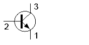
In the figure shown, 2 represents the
-
collector of a pnp transistor
-
emitter of an npn transistor
-
Correct Answerbase of an npn transistor
-
source of a junction FET
This question does not yet have an explanation!
Register to add one
In the figure shown, 3 represents the
-
drain of a junction FET
-
Correct Answercollector of an npn transistor
-
emitter of a pnp transistor
-
base of an npn transistor
This question does not yet have an explanation!
Register to add one
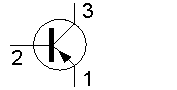
In the figure shown, 2 represents the
-
Correct Answerbase of a pnp transistor
-
drain of a junction FET
-
gate of a junction FET
-
emitter of a pnp transistor
This question does not yet have an explanation!
Register to add one
In the figure shown, 1 represents the
-
collector of a pnp transistor
-
gate of a junction FET
-
source of a MOSFET
-
Correct Answeremitter of a pnp transistor
This question does not yet have an explanation!
Register to add one
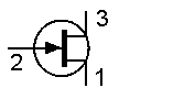
In the figure shown, 2 represents the
-
drain of a p-channel junction FET
-
collector of an npn transistor
-
Correct Answergate of an n-channel junction FET
-
base of a pnp transistor
This question does not yet have an explanation!
Register to add one
In the figure shown, 3 represents the
-
source of an n-channel junction FET
-
gate of a p-channel junction FET
-
emitter of a pnp transistor
-
Correct Answerdrain of an n-channel junction FET
This question does not yet have an explanation!
Register to add one
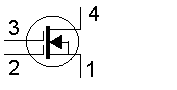
In the figure shown, 2 represents the
-
Correct Answergate of a MOSFET
-
base of a dual bipolar transistor
-
anode of a silicon controlled rectifier
-
cathode of a dual diode
This question does not yet have an explanation!
Register to add one
The figure shown represents a
-
dual bipolar transistor
-
dual diode
-
dual varactor diode
-
Correct Answerdual gate MOSFET
This question does not yet have an explanation!
Register to add one
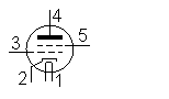
In the figure shown, 3 represents the
-
filament of a tetrode
-
anode of a triode
-
Correct Answergrid of a tetrode
-
screen grid of a pentode
This question does not yet have an explanation!
Register to add one
In the figure shown, 5 represents the
-
grid of a tetrode
-
Correct Answerscreen grid of a tetrode
-
heater of a pentode
-
grid of a triode
This question does not yet have an explanation!
Register to add one